Last quarter, a U.S. buyer sent us a batch of 5G connector housings that failed signal integrity testing—every single piece. The root cause? A 0.03 mm tolerance drift nobody caught at the source factory.
5G stamping parts require ultra-tight dimensional tolerances of ±0.01–0.05 mm and EMI shielding effectiveness of 40–60 dB attenuation to maintain signal integrity at millimeter-wave frequencies. Material selection, surface conductivity, burr-free edges, and thermal management are equally critical for compliance and high-frequency performance.
This article breaks down what purchasing managers need to specify, verify, and control when sourcing 5G stamping parts from Asia. We will cover tolerances by component type, shielding standards, material choices, and quality verification methods.
How do I ensure tight tolerances when sourcing 5G stamping parts from Asia?
A lesson we learned the hard way: sending a 2D drawing to a supplier and expecting ±0.01 mm results without a detailed GD&T callout and process capability study 1 is a recipe for rejected shipments and costly rework.
To ensure tight tolerances, specify GD&T callouts per component type, require Cpk ≥ 1.67 for critical dimensions, mandate progressive die stamping with in-process SPC, and verify capability through PPAP submissions before mass production begins.
Why Tolerances Differ by Component
Not every 5G stamped part needs the same precision level. The function of the part dictates how tight the tolerance must be. A mounting bracket can live with ±0.05 mm. A semiconductor lead frame cannot. Here is a breakdown we use internally when reviewing customer drawings:
| Component Type | Typical Tolerance | Why It Matters |
|---|---|---|
| Connector Housing / Waveguides | ±0.05 mm | Maintains RF signal integrity and mating fit |
| Semiconductor Lead Frames | ±0.002 mm (2 microns) | A 0.5-micron deviation causes up to 15% signal loss |
| Terminals & Contact Pins | ±0.003 mm | Prevents poor contact and intermittent connections |
| Shielding Cases / Enclosures | ±0.01–0.02 mm | Ensures gap-free Faraday cage for EMI/RFI shielding effectiveness |
| General Structural Brackets | ±0.05–0.10 mm | Mechanical fit only; less impact on signal |
A deviation of just half a micron on a high-frequency chip terminal 2 can destroy 15% of its signal capacity. That is not a theoretical number—it is a measurable, repeatable failure mode at millimeter-wave frequencies above 24 GHz.
Progressive Die Stamping and Micro-Stamping Technology
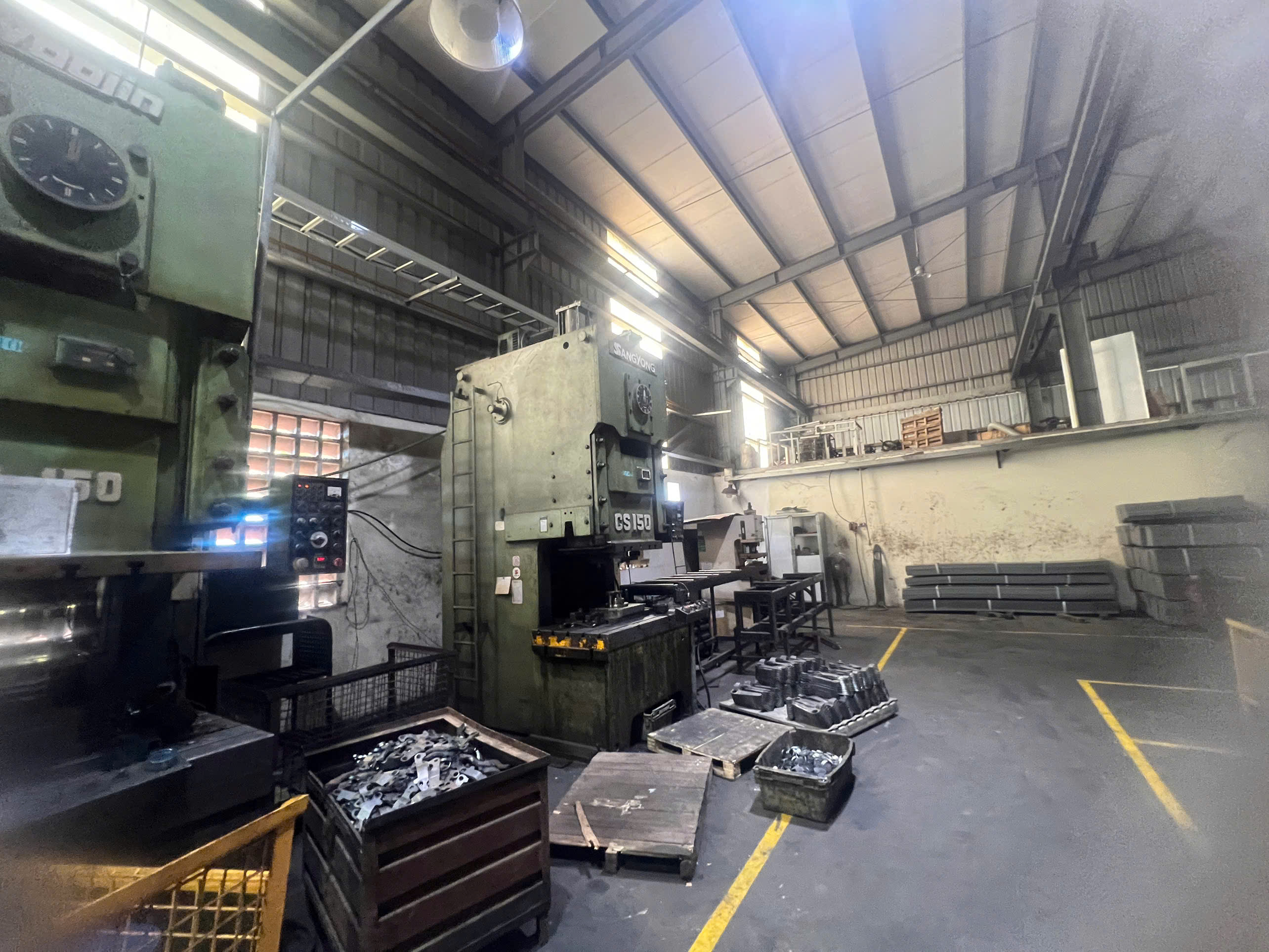
For volumes in the hundreds of thousands, progressive die stamping 3 is the only cost-effective way to hold 5-micron tolerances repeatedly. Our engineering team reviews die designs before tool steel is even cut. We verify the die material—specialized powder metallurgy tool steels are required to ensure sub-micron edge consistency across long production runs.
Micro-stamping technology becomes essential when parts drop below 0.2 mm thickness. Conventional dies simply cannot produce burr-free edges on ultra-thin sheets. Fine blanking or chemical etching must supplement the stamping process.
Practical Steps for Buyers
- Define critical-to-quality (CTQ) dimensions on your drawing. Not every dimension needs ±0.01 mm.
- Request a process capability study (Cpk) for those CTQ features before signing off on production.
- Include a PPAP requirement in your purchase order. This forces the supplier to prove they can hold tolerances before shipping a single production piece.
- Specify SPC monitoring for key dimensions during the run. Ask for X-bar and R charts 4 weekly.
When we manage sourcing projects, we audit the supplier's measurement equipment first. If they lack a CMM or optical comparator rated to the tolerance level required, that is an immediate red flag. You cannot inspect what you cannot measure.
Design Considerations That Protect Precision
Holes placed too close to bends will distort. The rule of thumb: keep holes at least 2× material thickness away from any bend line. Springback is another persistent challenge—especially with beryllium copper alloys 5 and phosphor bronze. The supplier must compensate for springback in the die design, not hope it resolves itself.
What shielding and EMI control standards should I require from my 5G parts supplier?
During a recent supplier audit in Vietnam, we tested a batch of shielding cans with a spectrum analyzer. They measured 35 dB attenuation—well below the 40 dB minimum. The cause was a 5-micron gap along one seam acting as a slot antenna, radiating mmWave energy right through the enclosure.
Require stamped shielding parts to meet 40–60 dB attenuation across 20–50 GHz bands, comply with IEC 61000 and FCC Part 15 standards, maintain 360° Faraday cage integrity with seam gaps below 3 μm, and achieve flatness of ≤0.002 mm/m to prevent signal leakage.
Understanding the Shielding Imperative
5G infrastructure operates at frequencies from sub-6 GHz up to 50 GHz for mmWave bands. At these frequencies, even a hairline gap in a shielding enclosure becomes a slot antenna. The electromagnetic wave does not just leak—it radiates. This is why EMI/RFI shielding effectiveness is not just a design preference; it is a regulatory gate.
The IEC 61000 series 6 governs electromagnetic compatibility (EMC) for electronic equipment. FCC Part 15 sets emission limits for unintentional radiators in the United States. If your 5G stamped enclosure does not meet these standards, you cannot sell the final product in the U.S. or EU markets.
Attenuation Requirements by Application
| Application | Minimum Attenuation | Frequency Range | Key Material |
|---|---|---|---|
| 5G Base Station Shielding | ≥60 dB | 20–50 GHz | Aluminum alloy |
| Small Cell Enclosures | 40–50 dB | 3.5–28 GHz | Aluminum or tin-plated steel |
| IoT Sensor Modules | 40–50 dB | 30–300 MHz (low-freq) | Copper alloy |
| Antenna-in-Package (AiP) Shields | ≥50 dB | 24–39 GHz | Ultra-thin copper or mu-metal |
Aluminum shields ≥85% of high-frequency EMI in the 20–50 GHz range. Copper performs better at lower frequencies, specifically in the 30–300 MHz band common in IoT sensors. The material choice is not interchangeable—it depends on the frequency band your product operates in.
The Dual Role: Shielding and Thermal Management
Metal stamped shields provide 50% better heat dissipation than polymer alternatives. For 5G radio units drawing 500–1,500 watts, thermal management is not optional. A stamped aluminum shield serves as both an electromagnetic barrier and a heat sink. Some designs integrate high-density thermal dissipation fins directly into the stamped form, eliminating the need for a separate heat sink.
This dual-role capability is a major reason metal stamping remains the preferred process for 5G enclosures despite the rise of die-cast and injection-molded alternatives.
Structural Requirements for Gap-Free Shielding
- Cut-edge burrs must be ≤3 μm. Anything larger creates micro-gaps that compromise shielding.
- Flatness must hold to ≤0.002 mm/m. Warped panels create air gaps when assembled.
- The enclosure must provide 360° coverage. Any opening, slot, or seam must be designed with overlapping flanges or conductive gaskets.
We always flag seam geometry during design reviews. A poorly designed joint can turn a compliant enclosure into a non-compliant one, and the problem will not show up until EMC testing—when the cost of correction is highest.
Which material and coating choices best meet 5G precision and shielding needs?
One trade-off we weigh on nearly every 5G project: beryllium copper gives outstanding spring performance and conductivity, but it costs three to five times more than phosphor bronze 7. The buyer's frequency band, mechanical cycle requirement, and budget must all be on the table before we recommend a material.
Beryllium copper alloys, phosphor bronze, and aluminum 5052 are the top base materials for 5G stamping parts. Selective silver-over-nickel plating optimizes surface conductivity at mmWave skin depths, while surface roughness must be held to Ra ≤ 0.2 μm for reliable high-frequency performance.
Base Material Comparison
Choosing the right base material is the single most consequential decision in a 5G stamping project. Here is how the primary options compare:
| Property | Beryllium Copper (C17200) | Phosphor Bronze (C51000) | Aluminum 5052 |
|---|---|---|---|
| Electrical Conductivity | 22% IACS | 15% IACS | 35% IACS |
| Elastic Modulus | 128 GPa | 110 GPa | 70 GPa |
| Spring Life (cycles) | >100,000 | >5,000 | N/A (not spring use) |
| Frequency Shielding Strength | Excellent (broadband) | Good (mid-range) | Excellent (high-freq, ≥85% at 20–50 GHz) |
| Relative Cost | High (3–5×) | Moderate (baseline) | Low to moderate |
| Typical 5G Use | Contact springs, terminals | Connector pins, clips | Shielding cans, enclosures |
Beryllium copper alloys 8 are the gold standard for contact springs that must survive more than 5,000 insertion cycles while maintaining an elastic modulus of 100–120 GPa. Phosphor bronze is the workhorse for pins and clips where cost matters and cycle life requirements are moderate. Aluminum 5052 dominates shielding applications because of its high conductivity-to-weight ratio and excellent high-frequency attenuation.
Material Thickness and Its Impact
5G stamping parts span a wide range of material thicknesses:
- Ultra-thin (below 0.2 mm): Required for package-level shielding (AiP) and precision contacts. These cannot be stamped with conventional dies—fine blanking or chemical etching is necessary.
- Thin gauge (0.2–1.0 mm): The most common range for terminals, enclosures, and connector housings. Standard high-precision progressive dies handle this well.
- Miniature/wearable (0.02–0.1 mm): Emerging demand for IoT sensors and wearable 5G devices. This range demands specialized micro-stamping technology and extremely rigid process controls.
Material quality matters as much as material type. The raw strip must have uniform yield strength, minimal directionality, high uniform elongation, and low work-hardening tendency. Without these properties, dimensional consistency across a production run is impossible.
Surface Finish and Plating for High-Frequency Performance
At frequencies above 24 GHz, the skin depth 9 of the electrical signal is extremely shallow—often just a few microns. This means the surface of the stamped part carries nearly all the current. Surface conductivity becomes the dominant factor in signal integrity.
Selective plating is the answer. A thin layer of silver over a nickel barrier 10 provides the best combination of conductivity and corrosion resistance for mmWave applications. The plating thickness must be optimized to match the skin depth at the operating frequency. Too thin, and the signal penetrates into the less conductive base metal. Too thick, and cost rises without benefit.
Surface roughness must be controlled to Ra ≤ 0.2 μm. Rough surfaces increase RF skin-effect losses, create hot spots, and can even cause electrical arcing in high-power applications. We always specify roughness limits on the drawing and verify them with a profilometer during PPAP.
Emerging Hybrid Approaches
Some advanced 5G enclosure designs now require hybrid co-stamping—metal shields with integrated dielectric inserts. These inserts provide localized impedance matching within the enclosure, improving signal routing without adding assembly steps. This is a growing trend we are seeing in requests from engineering design firms on the U.S. West Coast.
Post-stamping cryogenic stress-relief processes are also becoming more common. These treatments stabilize the dimensions of stamped parts that will face extreme outdoor thermal cycling—a real concern for 5G base station hardware exposed to desert heat or northern winters.
How do I verify my stamping supplier's quality control for 5G component consistency?
A buyer we work with in the Midwest once told us: "I don't care how good the first sample is. I care whether the ten-thousandth piece is identical." That single sentence captures everything about quality control for 5G stamping parts.
Verify your supplier's quality control by requiring PPAP with full dimensional reports, mandating SPC with Cpk ≥ 1.67 on critical features, conducting on-site audits of measurement equipment and die maintenance schedules, and insisting on 100% visual inspection for burr-free edges and surface defects.
The PPAP Foundation
Production Part Approval Process (PPAP) is non-negotiable for 5G stamping parts. It is the documented proof that a supplier can produce parts that meet your specifications consistently. A proper PPAP submission includes:
- Dimensional measurement reports on all CTQ features.
- Material certifications (mill certs) verifying alloy composition and mechanical properties.
- Process flow diagrams showing each stamping, plating, and inspection step.
- Control plans identifying what is measured, how often, and what the reaction plan is when something drifts.
- Initial process capability study (Cpk) demonstrating statistical control.
When we manage a project, we do not accept a PPAP that was self-reported by the factory. Our local team in Vietnam or China performs an independent dimensional verification using calibrated instruments. This catches discrepancies before the first container ships.
SPC and In-Process Monitoring
Statistical Process Control keeps tolerances in check during the run, not just at the start and end. For a 5G terminal with a ±0.003 mm tolerance, the process must be monitored continuously. X-bar and R charts track the mean and range of critical dimensions over time. Any trend toward the control limit triggers an adjustment before parts go out of spec.
High-speed stamping at 500–1,500 pieces per minute introduces unique challenges. Tool wear accumulates quickly. Springback can shift as the strip material changes between coils. Without SPC, these drifts go unnoticed until final inspection—by which time thousands of non-conforming parts may already be produced.
What to Look For During a Supplier Audit
We have conducted dozens of supplier audits specifically for precision stamping. Here is what separates a capable 5G supplier from a generic one:
- Measurement equipment: Do they have CMMs, optical comparators, and profilometers rated to the tolerance level you need? A shop that measures in hundredths of a millimeter cannot guarantee thousandths.
- Die maintenance records: Progressive dies wear. A good supplier tracks punch counts and has scheduled preventive maintenance intervals. Ask to see the logs.
- Tool steel grade: Specialized powder metallurgy tool steels (such as ASP23 or similar) are required for sub-micron edge consistency. If the supplier uses standard D2 tool steel, edge quality will degrade faster in high-volume runs.
- Environmental controls: Temperature fluctuations in the stamping shop cause dimensional drift in both the die and the material. Climate-controlled production areas are a sign of a serious precision operation.
- Burr inspection protocol: Burrs must be ≤3 μm for shielding parts. Ask how they inspect for burrs—visual? Microscope? Automated optical inspection? The answer tells you a lot about their quality culture.
Final Inspection and Shipping Controls
Even with SPC in place, a final inspection gate is essential. We use AQL sampling plans per ANSI/ASQ Z1.4, typically at Level II with a 0.65 AQL for critical defects. For 5G parts where signal integrity is at stake, we sometimes tighten this to 0.25 AQL or even implement 100% inspection on critical dimensions.
Packaging also matters. Precision parts that shift and rub against each other during transit develop surface scratches and edge damage. We specify anti-static trays, individual cavity packaging, or foam-lined containers depending on the part geometry and surface finish requirements.
Conclusion
5G stamping parts demand precision and shielding that go far beyond standard metal stamping. Specify tolerances by component function, verify EMI attenuation against IEC and FCC standards, choose materials matched to your frequency band, and audit your supplier’s process controls before production begins.
Frequently Asked Questions
How do I ensure tight tolerances when sourcing 5G stamping parts from Asia?
A lesson we learned the hard way: sending a 2D drawing to a supplier and expecting ±0.01 mm results without a detailed GD&T callout and process capability study 1 is a recipe for rejected shipments and costly rework.
What shielding and EMI control standards should I require from my 5G parts supplier?
During a recent supplier audit in Vietnam, we tested a batch of shielding cans with a spectrum analyzer. They measured 35 dB attenuation—well below the 40 dB minimum. The cause was a 5-micron gap along one seam acting as a slot antenna, radiating mmWave energy right through the enclosure.
Which material and coating choices best meet 5G precision and shielding needs?
One trade-off we weigh on nearly every 5G project: beryllium copper gives outstanding spring performance and conductivity, but it costs three to five times more than phosphor bronze 7 . The buyer's frequency band, mechanical cycle requirement, and budget must all be on the table before we recommend a material.
Footnotes
1. Wikipedia entry explaining the statistical calculation of process capability indices like Cpk. ↩︎
2. Industry leader page explaining the role of lead frames and terminals in semiconductor packaging. ↩︎
3. Technical resource from a leading manufacturer of precision stamping tool components. ↩︎
4. NIST engineering statistics handbook explains X-bar and R control chart methodology used in SPC. ↩︎
5. Copper Development Association provides authoritative data on copper alloy properties and applications. ↩︎
6. IEC official site details the 61000 series standards governing electromagnetic compatibility compliance. ↩︎
7. Wikipedia page covering the composition and industrial applications of phosphor bronze alloys. ↩︎
8. Manufacturer product page detailing the mechanical and electrical properties of beryllium copper. ↩︎
9. Academic explanation of the skin effect and skin depth at high frequencies. ↩︎
10. Industry article discussing the role of nickel plating as a barrier layer. ↩︎