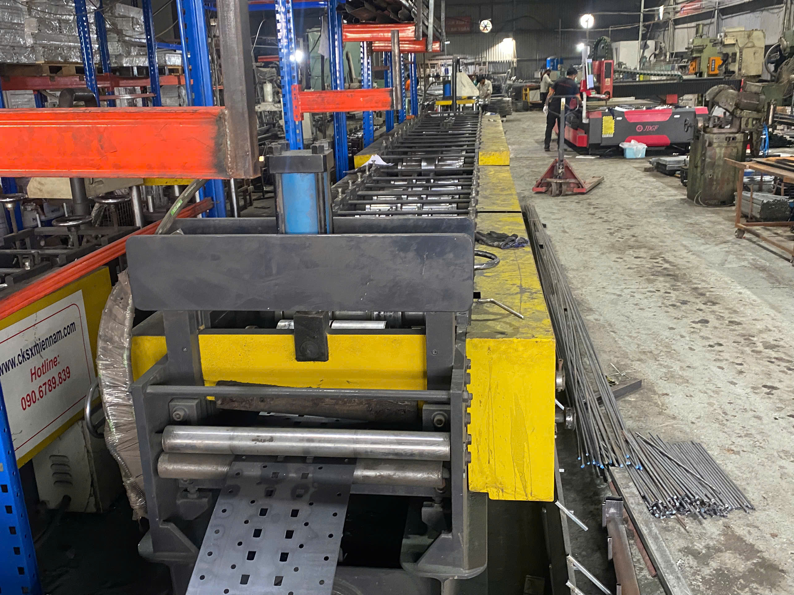
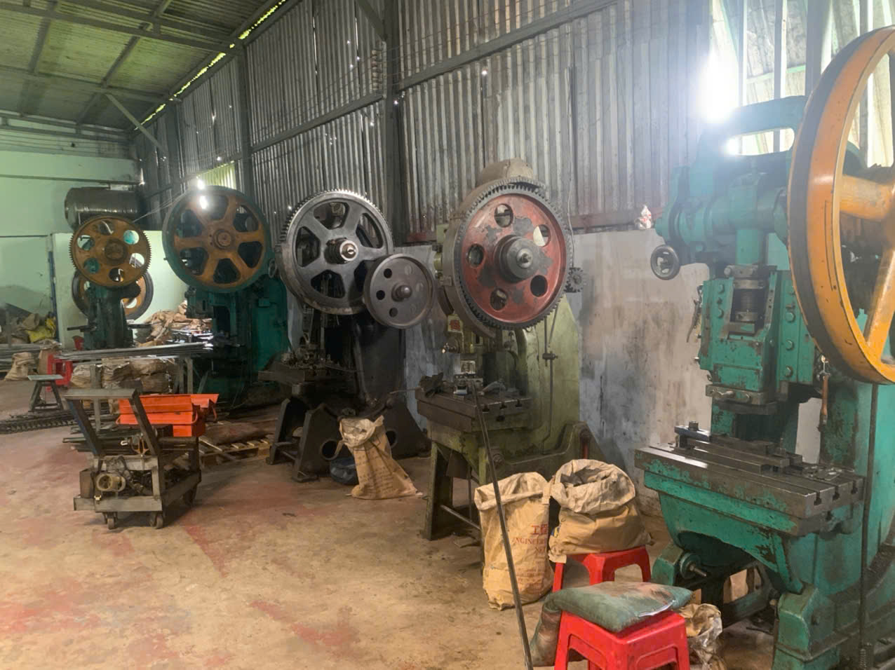
Stamping parts in consumer electronics rarely get noticed until one fails EMI shielding 1. On our supply chain projects, a single bad battery contact has stalled entire production runs for our U.S. clients.
Stamping parts play a foundational role in consumer electronics by providing electrical connectivity, structural support, EMI shielding, and heat dissipation. Stamped connectors, contacts, brackets, shielding cans, and heat sinks enable devices to stay compact, reliable, and affordable in high-volume production.
Let me walk you through the parts that matter most, the quality standards to demand, the materials to specify, and how to find a supplier who actually delivers on time.
How can I identify which stamping parts are critical for my consumer electronics designs?
A while back, our engineers tore down a client's Bluetooth speaker to map every stamped component inside it ISO 2. We counted seventeen. The client had only flagged four as critical.
Critical stamping parts in consumer electronics include battery contacts, connectors, terminals, EMI shielding cans, antenna components, structural frames, brackets, and heat sinks. Any stamped part that carries current, blocks interference, or manages heat should be classified as critical and controlled tightly.
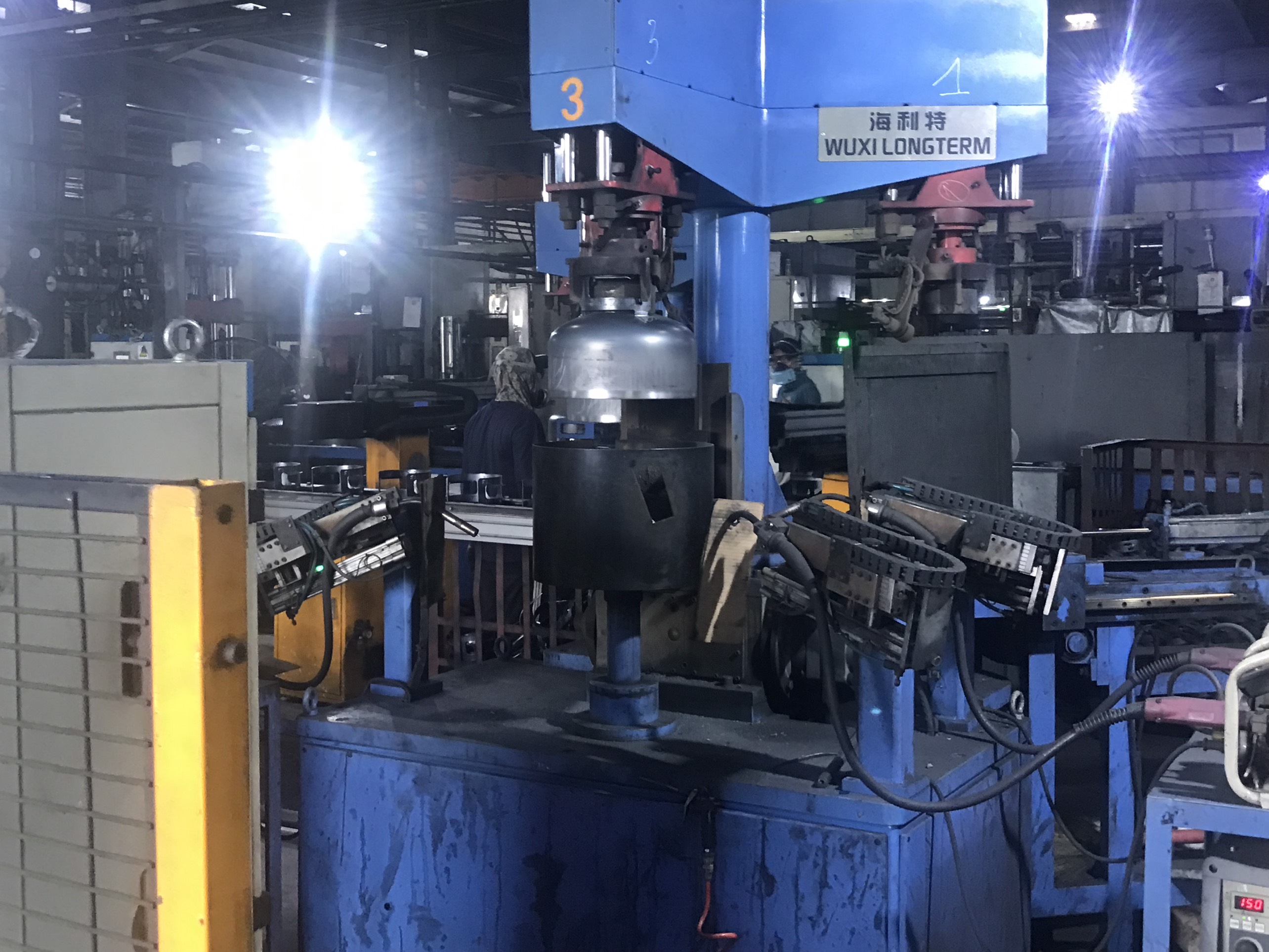
Most buyers underestimate how many stamped parts sit inside a single device supply chain 3. In our sourcing work, we teach clients to sort stamped components by function first, then by risk. A decorative trim clip is not the same as a grounding spring. If the part carries current, shields circuitry, or moves heat, it deserves critical status.
Sort parts by their function
Start with a simple functional map of your device. Here is the framework we use during design reviews with our engineering clients:
| Function | Typical Stamped Parts | Failure Impact |
|---|---|---|
| Electrical connectivity | Battery contacts, terminals, connector pins, charging port springs | Device will not power on or charge |
| EMI/RF shielding | Shielding cans, ground clips, antenna elements | Signal interference, failed compliance testing |
| Structural support | Frames, brackets, chassis parts, camera lens holders | Assembly misalignment, drop-test failure |
| Thermal management | Stamped heat sinks, thermal spreaders | Overheating, throttling, shortened lifespan |
Score the risk, not just the price
Cheap parts can carry high risk. A stamped battery spring might cost a few cents, but if it loses contact force after thermal cycling, the whole device fails in the field. We ask three questions for every stamped part: Does it touch the electrical path? Does it affect regulatory compliance? Does it hold tolerance-sensitive components in place? One "yes" makes it critical.
By device type, the priorities shift. Smartphones lean heavily on antenna parts, shielding, and micro-contacts. Laptops need thermal stampings and connector hardware. Wearables depend on tiny battery contacts and spring terminals where thickness can drop below 0.2 mm. Map your own product this way before you write a single purchase order.
What quality control standards should I require when sourcing stamping parts for electronics manufacturing?
One of our U.S. purchasing clients once received a full container of brackets with one hole punched 0.3 mm off-position. The prior supplier had no first-article inspection. We rebuilt his QC process from scratch.
Require first-article inspection, PPAP documentation, in-process SPC monitoring, dimensional reports against the drawing, material certificates, plating thickness verification, and final AQL-based inspection. For micro-precision electronics stampings, add automated optical inspection and in-die sensor monitoring to catch defects at the press.
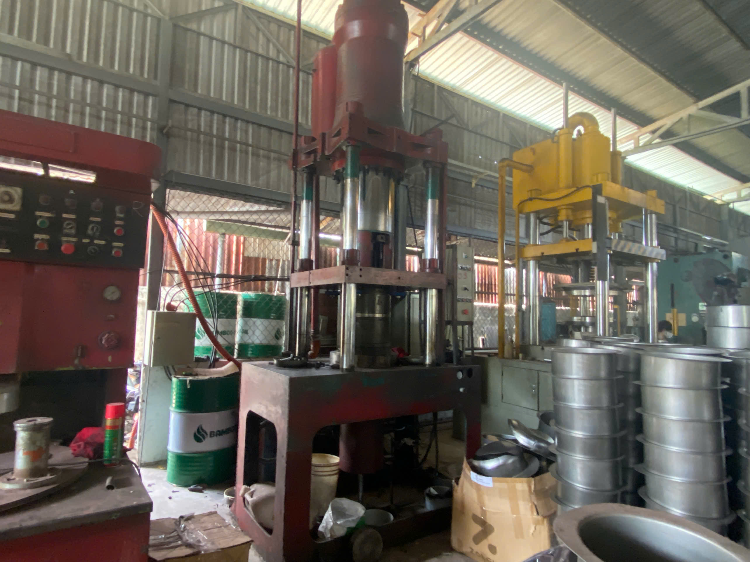
Quality control for electronics stampings is not one checkpoint. It is a chain of gates from raw material to shipped carton. When we run supplier audits across Vietnam and other Asian countries, we look for evidence at every gate, not promises.
The QC gates we enforce
- Incoming material verification. Check mill certificates for alloy grade, temper, and thickness. Wrong temper means wrong spring force, even if dimensions look perfect.
- First-article inspection (FAI). Measure every drawing dimension on the first parts off the die. Approve nothing until the FAI report matches the print.
- PPAP submission. For production launch, we require a full production part approval package: control plans, process flow, measurement system analysis, and capability studies.
- In-process monitoring. Progressive stamping runs fast. Statistical process control 4 on key dimensions catches die wear before it produces scrap.
- Plating and finish checks. Verify plating thickness, adhesion, and solderability where the drawing calls for it. Corrosion resistance depends on it.
- Final inspection to AQL. Sample against an agreed AQL level before packing, with a documented report your team can review before the goods ship.
Modern tools worth demanding
For sub-100-micron tolerance work, manual calipers are not enough. Ask whether the supplier runs automated optical inspection (AOI) on the line and in-die sensors that stop the press when a misfeed occurs. In our experience, factories that invest in these tools deliver "right first time" far more consistently than those relying on end-of-line sorting.
Document everything in writing before the tooling kickoff. A drawing note that is not in the control plan will be missed. That is the single most common root cause of non-conforming stampings we see.
Which materials and tolerances matter most when I order custom stamping parts for consumer devices?
There is a trade-off we weigh on almost every electronics stamping quote: conductivity versus spring performance. Pure copper conducts beautifully but fatigues quickly. Beryllium copper 5 holds its spring but costs more. The drawing has to choose.
The most important materials are copper alloys and beryllium copper for contacts, stainless steel for structural and spring parts, and aluminum for shields and heat sinks. Critical tolerances include contact positions, bend angles, flatness, and hole locations, often held within ±0.02–0.05 mm.
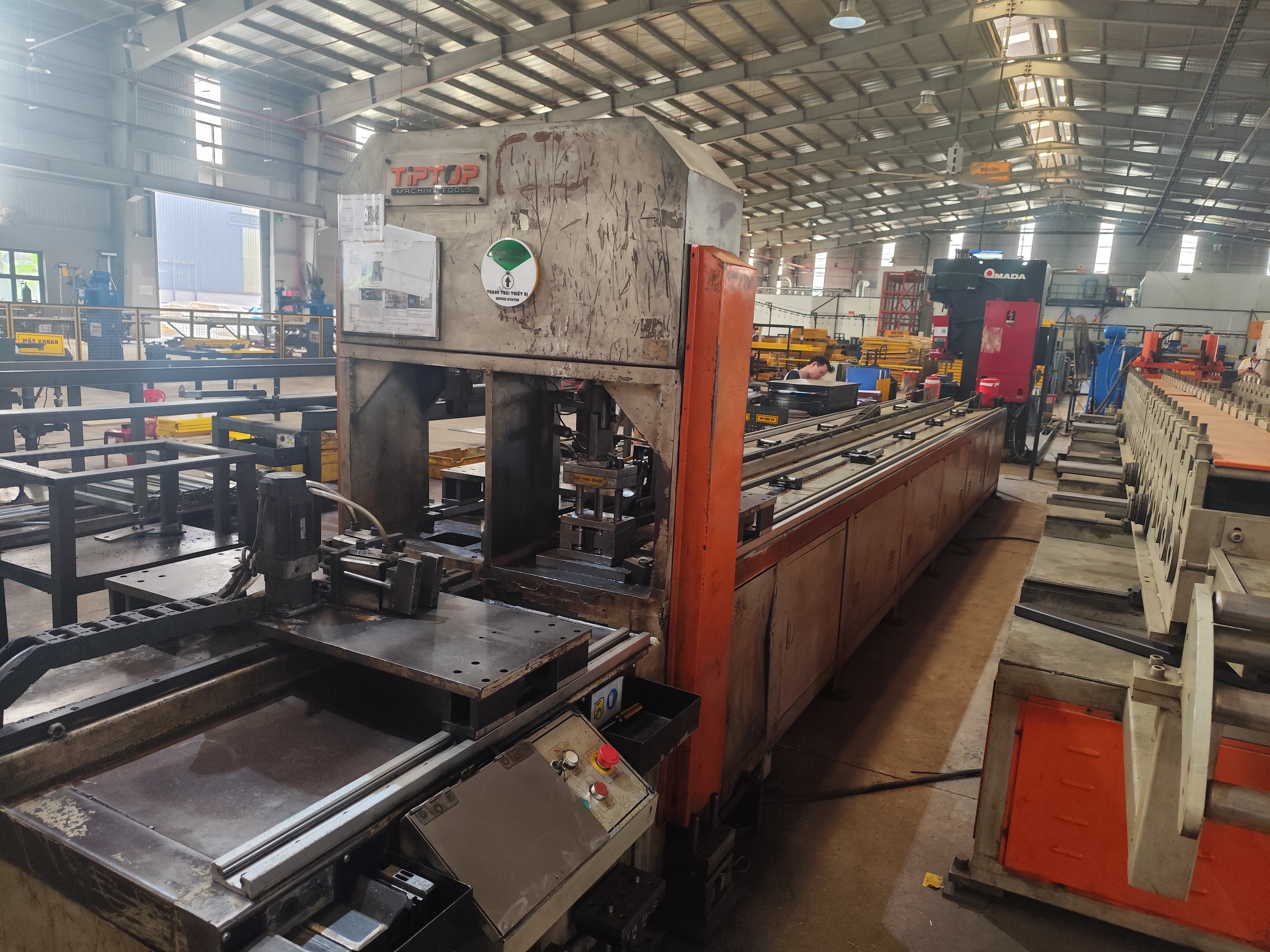
Material choice drives everything downstream: conductivity, spring force, corrosion behavior, solderability, and cost. When our team in Singapore reviews a new drawing, material and tolerance callouts are the first two things we check, because they determine which factories can even quote the job.
Matching material to function
| Material | Best Use in Electronics | Key Properties | Watch Out For |
|---|---|---|---|
| Copper alloys (brass, phosphor bronze) | Connectors, terminals, contacts | High conductivity, good formability | Moderate spring fatigue over cycles |
| Beryllium copper | Battery springs, RF contacts, 5G antenna parts | Excellent spring properties plus conductivity | Higher cost, special handling |
| Stainless steel 6 | Frames, brackets, clips, shielding | Strength, corrosion resistance | Lower conductivity, harder on dies |
| Aluminum | Heat sinks, shielding cans, enclosures | Lightweight, good thermal transfer | Softer, prone to scratches |
Tolerances that actually matter
Not every dimension needs to be tight. Over-toleranced drawings inflate cost and lengthen lead times. In our co-development projects, we push clients to tighten only what the function demands:
- Contact point position: determines whether the part mates reliably; typically the tightest callout on the print.
- Bend angles: control spring force and assembly fit; small angle errors compound across multiple bends.
- Flatness and coplanarity: critical for SMT-compatible parts that must sit flat on the PCB during reflow.
- Hole and slot locations: drive assembly alignment with screws, posts, and mating components.
- Material thickness consistency: micro-precision parts below 0.2 mm thickness leave almost no margin for coil variation.
Plating deserves equal attention. Nickel underplating with tin or gold flash is common for solderable contacts. Specify plating thickness ranges on the drawing, not just "gold plated." Vague finish callouts cause more disputes between buyers and Asian factories than any dimensional issue we handle.
How do I find a reliable stamping parts supplier in Asia who can meet my electronics production deadlines?
The hardest lesson I learned early in our export business was this: a factory that quotes fast is not the same as a factory that delivers fast. Our Vietnam office now exists partly because we needed eyes on the ground to verify real capacity.
Find a reliable Asian stamping supplier by auditing their tooling capability, press capacity, and QC systems on-site, requesting PPAP samples before commitment, checking references from electronics clients, and confirming realistic lead times in writing. A local presence or sourcing partner in-region dramatically reduces delivery risk.
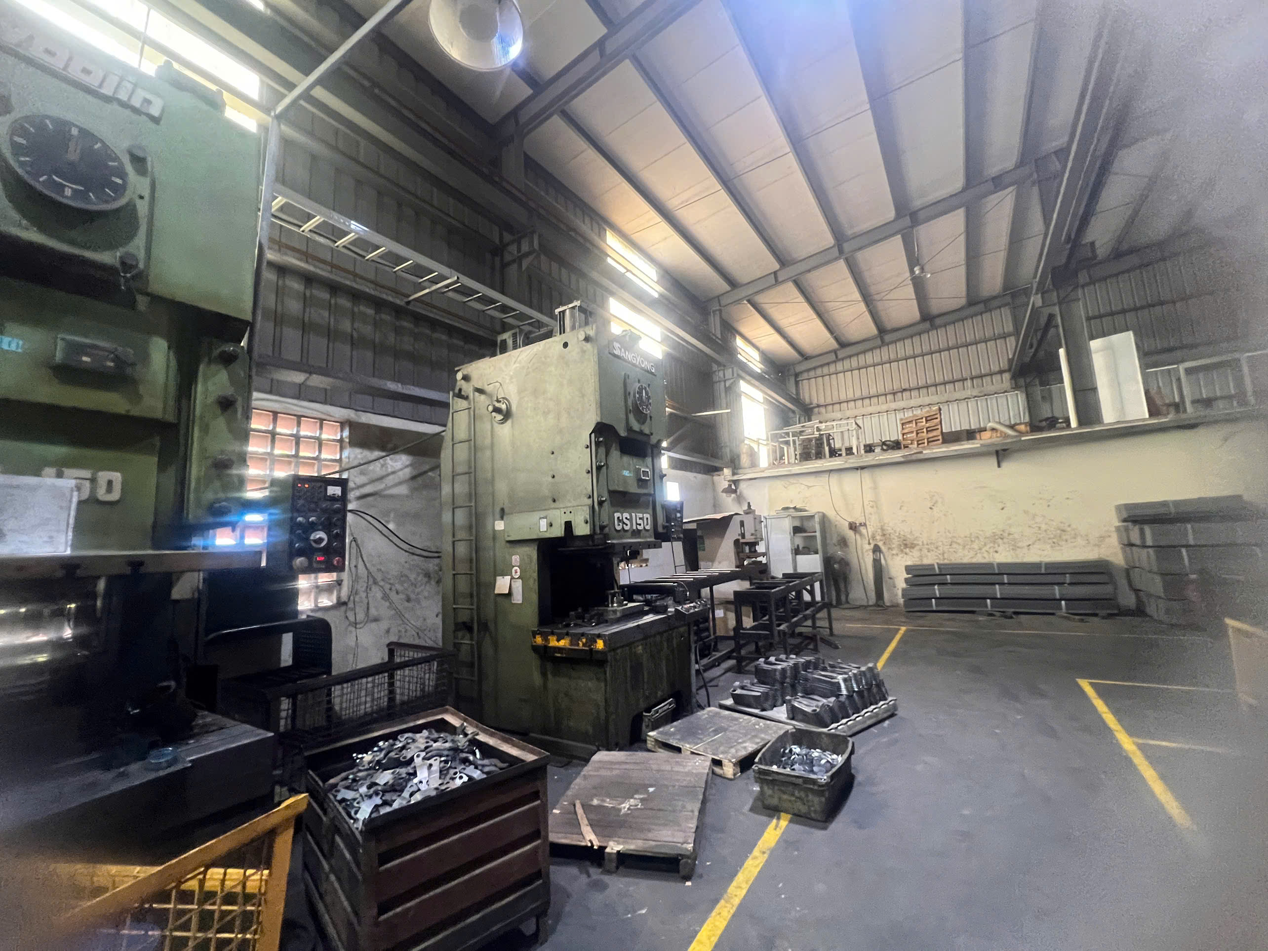
Deadlines slip for predictable reasons: overloaded presses, delayed tooling, material shortages, and failed first articles that force rework. Each risk can be checked before you place the order. Here is the vetting sequence we run for our U.S. clients sourcing across Vietnam, Taiwan, India, and other Asian countries World Trade Organization 7.
A practical supplier vetting checklist
| Vetting Step | What to Verify | Red Flag |
|---|---|---|
| Factory audit | Press tonnage range, tool room in-house, maintenance records | Outsourced tooling with no schedule control |
| Capacity check | Current utilization, shift structure, order backlog | "We can always fit you in" with no data |
| QC system review | FAI process, SPC records, AOI equipment, calibration logs | Inspection reports written after shipping |
| Sample and PPAP stage | Dimensional reports matching your drawing exactly | Samples that "mostly" conform |
| Reference checks | Existing electronics clients, export experience | Only domestic or non-electronics customers |
| Commercial terms | Written lead times, penalty clauses, payment terms | Verbal promises only |
Why local presence changes the game
Email alone cannot manage a stamping project across time zones. When a die cracks mid-run, someone needs to be at the factory within a day, not negotiating over a video call a week later. Our teams in Vietnam and China visit factories during tooling trials, witness first-article measurements, and perform final inspections before containers close. That physical presence is why our clients see far fewer surprises at their receiving dock.
Also weigh the commercial side. Suppliers or sourcing partners offering open account terms ease your cash flow during ramp-up, which matters when tooling investment and first production orders land in the same quarter. Confirm door-to-door logistics responsibility in the contract too. A stamped part that arrives late is a failed part, no matter how perfect its dimensions.
Conclusion
Stamping parts quietly enable every compact device: connecting power, shielding signals, and moving heat. Specify them precisely, control quality at every gate, and vet your Asian supplier on-site before committing.
Frequently Asked Questions
How can I identify which stamping parts are critical for my consumer electronics designs?
A while back, our engineers tore down a client's Bluetooth speaker to map every stamped component inside it ISO 2 . We counted seventeen. The client had only flagged four as critical.
What quality control standards should I require when sourcing stamping parts for electronics manufacturing?
One of our U.S. purchasing clients once received a full container of brackets with one hole punched 0.3 mm off-position. The prior supplier had no first-article inspection. We rebuilt his QC process from scratch.
Which materials and tolerances matter most when I order custom stamping parts for consumer devices?
There is a trade-off we weigh on almost every electronics stamping quote: conductivity versus spring performance. Pure copper conducts beautifully but fatigues quickly. Beryllium copper 5 holds its spring but costs more. The drawing has to choose.
Footnotes
1. Wikipedia explains electromagnetic interference shielding concept referenced throughout the article. ↩︎
2. ISO is the standards body relevant to quality management systems referenced in QC processes. ↩︎
3. Wikipedia background on supply chain concept central to the article’s manufacturing sourcing context. ↩︎
4. Wikipedia background on SPC methodology used for in-process quality monitoring. ↩︎
5. Wikipedia provides material science background on this alloy used in electronic contacts. ↩︎
6. Wikipedia background on material properties relevant to structural stamping parts. ↩︎
7. Authoritative trade body relevant to cross-border sourcing and manufacturing discussed in the article. ↩︎